At WiseGEEK, we're committed to delivering accurate, trustworthy information. Our expert-authored content is rigorously fact-checked and sourced from credible authorities. Discover how we uphold the highest standards in providing you with reliable knowledge.
What is Nanofabrication?
 Michael Anissimov
Michael Anissimov
Michael Anissimov
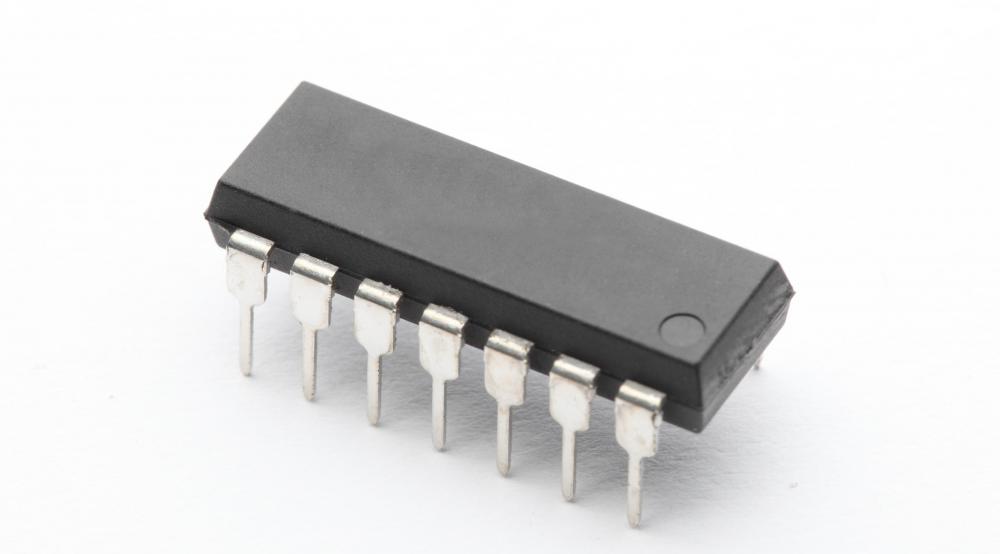
"Nanofabrication" refers to the fabrication of structures with feature sizes measured in the nanometers, especially below 20 nanometers on a side. Current technology mostly permits nanofabrication only in a two-dimensional sense. A major subset of current nanofabrication are the technologies that fall under the purview of nanolithography, which basically just means "nano-scale writing" and implies a 2-dimensional result. In this sense, even conventional photolithography used to make computer chips is technically nanofabrication, as feature sizes are measured in the hundreds of nanometers. However, "nanofabrication" tends to refer to newer and more cutting-edge approaches.
Conventional photolithography, the mainstay of the computing industry, can be used to create features with dimensions as small as 22 nm, though this is very expensive and is not currently considered cost-effective. More typically, patterns have feature sizes of about 193 nm as a lower bound. In anticipation of running up against physical limits with photolithography, computer companies have invested billions of dollars in research for next-generation lithography techniques. These include x-ray lithography (feature sizes of 15 nm), double patterning (using a lower-resolution approach but patterning the same surface twice), electron-beam direct-write lithography (EBDW), extreme ultraviolet lithography, nanoimprint lithography, scanning probe lithography (which can manipulate individual atoms), and atomic force microscope nanolithography.

More advanced approaches to nanofabrication are molecular self-assembly, which has been demonstrated in the lab hundreds of times, or positional mechanosynthesis, which is at the earliest research stages. Both are attempts to take nanofabrication into the 3D realm, which would truly unlock its technological power. Fast-through nanofabrication in 3D would mean that manufacturers could theoretically build a wide range of chemically possible structures with nanometer precision. This could lead to engines orders of magnitude more powerful than today, materials with 100 times better strength-to-weight ratios, electronics embedded in everything, and more. For now, though, nanofabrication is mostly just used for making better computer chips.
Michael Anissimov
Michael is a longtime WiseGEEK contributor who specializes in topics relating to paleontology, physics, biology, astronomy, chemistry, and futurism. In addition to being an avid blogger, Michael is particularly passionate about stem cell research, regenerative medicine, and life extension therapies. He has also worked for the Methuselah Foundation, the Singularity Institute for Artificial Intelligence, and the Lifeboat Foundation.
Learn more...
Michael Anissimov
Michael is a longtime WiseGEEK contributor who specializes in topics relating to paleontology, physics, biology, astronomy, chemistry, and futurism. In addition to being an avid blogger, Michael is particularly passionate about stem cell research, regenerative medicine, and life extension therapies. He has also worked for the Methuselah Foundation, the Singularity Institute for Artificial Intelligence, and the Lifeboat Foundation.
Learn more...AS FEATURED ON:
AS FEATURED ON:

-
![Nanofabrication is often used to make computer chips.]() By: ing_masaNanofabrication is often used to make computer chips.
By: ing_masaNanofabrication is often used to make computer chips.
Discuss this Article
Post your comments